ESR12 – Sviatoslav Voskresenskyi – Basics of EMC: Scientific Background of Daily Issues
Have you ever noticed that strange buzzing that goes out from your PC’s speakers or portable radio preceding the nearly lying phone ringing? Perhaps, you noticed that tidying one part of your hose with a vacuum cleaner somehow related to the appearance of the distortions on the TV screen in another part of the house? Or maybe the USB connection between your PC and smartphone disrupts the linking of your wireless mouse or keyboard with the receiver installed on the computer box?
All the above accidents or rules do not seem to be coherent with each other at the first sight, at least they all are lying in the electricity domain. But, if we consider each case more closely it becomes apparent that respectively to every scenario, the signal we try to receive with whatever device, whether it is a TV, radio, or another wireless receiver, is obstructed. And those examples are just the tip of the iceberg of what is called electromagnetic interference or briefly EMI.
Knowing that we can formulate the EMI as a disturbance generated by an external source that affects other electronic devices and equipment intentionally or unintentionally.
At the first sight, the name electromagnetic interference might sound a bit off-putting for a non-prepared reader. If the “interference” part is understood, how could be deciphered the “electromagnetic”, or EM in short? The EM means nothing but a signal. So, let’s make some sense of the EM signal.
The EM signal (or EM radiation) consists of two main parts created by the variable magnetic field (caused by variable currents, like solenoids) and a variable electric field (caused by a variable magnetic field or by electric charges, like in a capacitor). The most common example of EM radiation you might come across is visible light. The radiation can be guided by the transmission path also known as an antenna or by free space. The propagation speed is equal to the speed of flight. The EM wave can be depicted as follow:
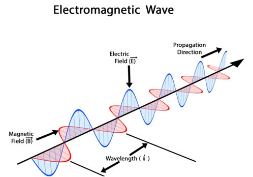
Schematiс Representation of EM wave[1]
There are also two important parameters each wave has: wavelength (λ) or the distance traveled by a wave in one full oscillation cycle, which varies from 100 million parts of a millimeter to hundreds of kilometers and frequency (f) which is several cycles per second with is equal to one Hertz. The graph below categorizes waves according to their frequency and length. As we mentioned before, visible light is also present in this chart.
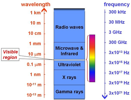
Visualization of the wavelength depending on frequency[2]
But there is one more parameter that describes how the wave will propagate through the different materials, or more scientifically – mediums: the characteristic impedance of the space on mere intrinsic impedance. Since we have only two main components of the wave (electric and magnetic components) the two parameters of a medium are interesting for us: permittivity – or natural electrical capacitance and permeability – natural electrical inductance. The ratio of those components determines the “resistance” of a medium. This is important to know if we want to protect our device with EM shields. The idea of the shield is to partially reflect the undesired EM wave and partially absorb it. And to determine the effectiveness of the shied we also need to know the properties of the wave or the wave impedance. Hence, while the intrinsic impedance describes the relations of permittivity and permeability, the wave impedance shows the correlation between the electric field and the magnetic field.
But, mostly, shielding is considered the last option in development thus the more appropriate attitude in deigning is to predict and eliminate all potential EMI sources in the early creation stage. In this case, we should have a look at the EM wave from another perspective: the space waveform.
All that was described as EM waves earlier is mostly truthful for planar waves, while emission tends to be formed in a spherical waveform. The form in its turn depends on how far from the emission source we observe the EM wave. It can be depicted as:
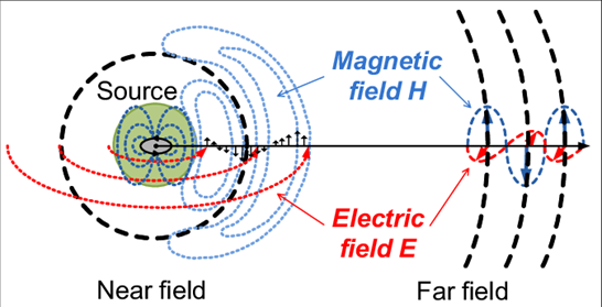
Representation of the spherical and planar waves around the EM source[3]
It’s quite easy to understand how the spherical waves become a planar form: the most apparent example is to compare the golf ball with the earth – both have the approximately same shape, but depending on the size and placement of the observer the sameness becomes not so evident.
By knowing the basic ideas of the EMI, exactly the source, the EM wave components, EM wave resistance, and EM wave shape how could it be used practically?
And here electromagnetic compatibility (EMC) science comes into play.
The EMC describes the ability of electronic devices to work together without obstructions. The EMC science can provide a wide range of solutions tended to reduce EMI in different applications, but the only way for applying the proper and effective solution is to understand what we are dealing with. The best way for that is to scan the emissions of the device. Accordingly, to the type of the wave, two different methods are applied.
The Far Field (FF) scanning is the method applied to understand the general properties of the emission from the device, thus providing feedback if the level of emission complies with the norms and laws of the country where a device has been intended to be used.
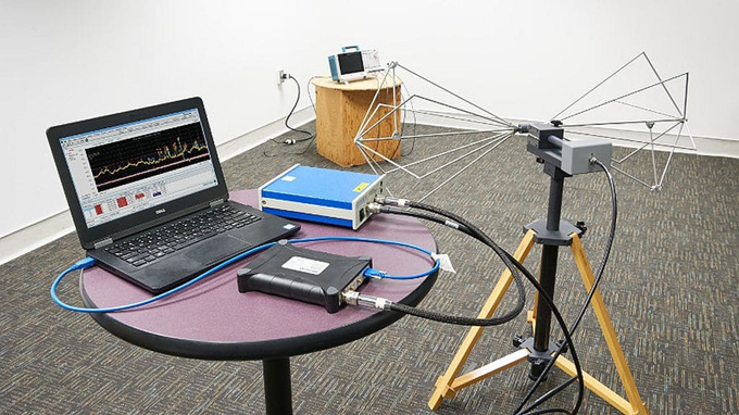
Far Field testing setup[4]
The Near Field (NF) scanning is used for finding the electric and magnetic emission sources in a system. This method is applied at the early stage of the development and allows analyzing and comparing design iterations for the further optimization of the device.
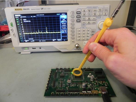
Near Field testing process[5]
Additionally, by applying several methods this type of testing could provide enough data to predict the far-field emissions of the device.
[1] Wikipedia, DECHAMMAKL, (9th February 2018), ಕನ್ನಡ: ಱ್ [online]. Available at: https://commons.wikimedia.org/wiki/File:Electromagnetic_waves.png [Accessed 25th April 2022]
[2] Swinburne University of Technology, [online]. Available at: https://astronomy.swin.edu.au/cosmos/e/electromagnetic+spectrum [Accessed 25th April 2022]
[3] Erik Jan Marinissen, Dae Young Lee2 John P. Hayes, Chris Sellathamby, Brian Moore, Steven Slupsky, Laurence Pujol
(April, 2009), Contactless Testing: Possibility or Pipe-Dream? ResearchGate [online]. Available at: https://www.researchgate.net/publication/221340771_Contactless_testing_Possibility_or_pipe-dream?enrichId=rgreq-e57695a9cd507c723c6b3102a8d09101-XXX&enrichSource=Y292ZXJQYWdlOzIyMTM0MDc3MTtBUzoxMDI3NTIzNTcxOTE2ODdAMTQwMTUwOTQ3OTQ0OA%3D%3D&el=1_x_2&_esc=publicationCoverPdf [Accessed 25th April 2022]
[4] Dylan Stinson (2nd March , 2020), How to Build Your Own EMI Troubleshooting and Pre-Compliance Kit, Interference Technology [online]. Available at: https://interferencetechnology.com/how-to-build-your-own-emi-troubleshooting-and-pre-compliance-kit/ [Accessed 25th April 2022]
[5] Rigol, (23rd December, 2014), EMC Precompliance Testing: Near Field Probing [online]. Available at: https://www.alldaq.com/fileadmin/user_upload/files/datasheets/rigol/Precompliance_Near_Field_Probing.pdf [Accessed 25th April 2022]

